Chapter 4 | The von Neumann Model
Basic Components
The instruction is the smallest piece of work specified in a computer program.
The von Neumann model consists of five parts : memory, a processing unit, input, output and a control unit.
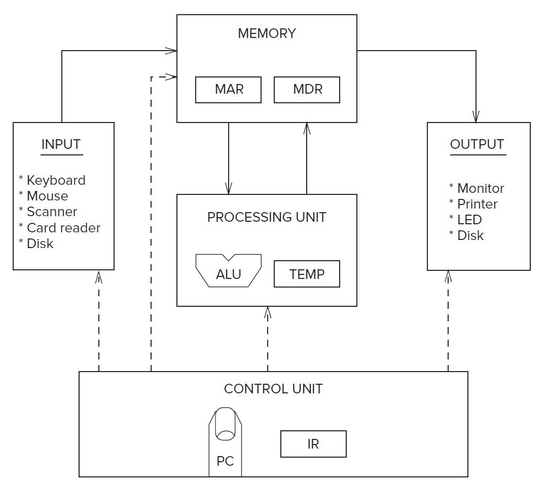
Memory
MAR is memory's address register.
MDR is memory's data register.
The value stored in the location can be changed, but the location's memory address remains unchanged.
Address space of LC-3 is 216 memory locations and LC-3 is 16-bit addressable.
TO READ / LOAD
- Load the address of the location in MAR.
- Interrogate the memory.
- The information stored in the corresponding location will be loaded in MDR.
TO WRITE / STORE
- Write the address of the memory location in the MAR and the value to be stored in the MDR.
- Interrogate the memory with the WE signal asserted.
- The information in the MDR will be stored into the corresponding location.
Processing Unit
Computation Unit
Definition
ALU is arithmetic and logic unit.
The ALU processes data elements of a fixed size referred to as the word length.
The data elements are called words.
Each ISA has its own word length. LC-3 has a word length of 16-bits.
Temporary Storage
The most common form of temporary storage is a set of registers
x86 microarchitectures have 8 registers. Some have 256 registers.
Input and Output (Peripherals)
In our course, we only use one input device keyboard and one output device monitor.
Control Unit
Definition
instruction register contains the instruction to be executed.
PC, program counter or say instruction counter, contains the next instruction's address to keep track of which instrcutions is to be processed next.
finite state machine
Instruction Processing
Instruction
There are fundamentally 3 kinds of instructions : operates, data movement and control.
Operate instructions operate the data. e.g. ADD and AND.
Data movement instructions move information from the processing unit to and from memory and to and from input/output devices. e.g. LD and ST.
Control instructions alter the sequential processing of instrcution. e.g. BR.
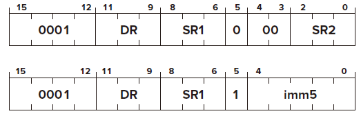
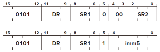
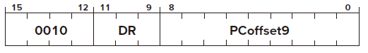
An LC-3 instruction consists of 16 bits (one word).
Bits [15:12] contain the opcode. Bits [11:0] are used to figure out where the operands are.
ADD
Opcode \(\text{[15:12]} = 0001\)
Operand
- \(\text{[11:9]}\) : DR (for destination register)
- \(\text{[8:6]}\) : SR1 (for source register 1)
- \(\text{[5]}\) : Signification digit
- register | if its value is
0,- the second operands is the value in SR2 specified by bits\(\text{[2:0]}\).
- \(\text{[4:3]}\) must be
0.
- register | if its value is
- immediate / literal | if its value is
1, - the second operand is obtained by sign-extending bits\(\text{[4:0]}\)to 16 bits.
FUNCTION
Condition Codes  : based on whether the result is negative, zero, or positive.
AND
Opcode \(\text{[15:12]} = 0101\)
Operand
- \(\text{[11:9]}\) : DR
- \(\text{[8:6]}\) : SR1
- \(\text{[5]}\) : Signification digit
- register | if its value is
0,- the second operands is the value in SR2 specified by bits\(\text{[2:0]}\).
- \(\text{[4:3]}\)must be
0.
- immediate / literal | if its value is
1,- the second operand is obtained by sign-extending bits \(\text{[4:0]}\) to 16 bits.
- register | if its value is
FUNCTION
Condition Codes : based on whether the result is negative, zero, or positive.
LD
Opcode \(\text{[15:12]} = 0010\)
Operand
- \(\text{[11:9]}\) : DR
- \(\text{[8:0]}\) : PCoffset (PC-Relative Mode)
FUNCTION
Condition Codes : based on whether the value loaded is negative, zero, or positive.
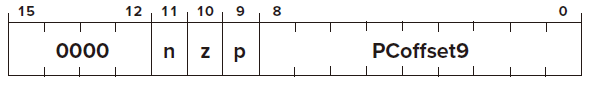
BR
Opcode \(\text{[15:12]} = 0000\)
Operand
- \(\text{[11:9]}\) : n, z, p (negative, zero, positive)
- if bits\(\text{[11]}\) is
1, N is tested. - if bits\(\text{[10]}\) is
1, Z is tested. - if bits\(\text{[09]}\) is
1, P is tested. - if any of the condition code tested is
1, the PC is loaded with the following address.
- if bits\(\text{[11]}\) is
- \(\text{[8:0]}\) : PCoffset (PC-Relative Mode)
FUNCTION
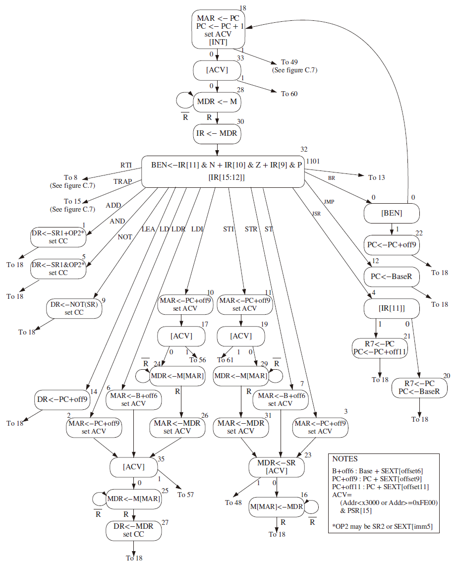
Instruction Cycle
Instruction Cycle is the entire sequence of steps needed to process an instruction. It consists of six sequential phases.
Every instruction consists FETCH and DECODE, but NOT all phases are needed for all instructions.
e.g. LD skips phase EXECUTE, ADD skips phase EVALUATE ADDRESS and FETCH OPERANDS.
1. FETCH
At least THREE clock cycles to complete. (Depend on the memory speed) 1. MAR is loaded with the contents of the PC, and simultaneously increment PC. 2. The memory is interrogated. (the next instruction specified by MAR is placed into MDR) 3. IR is loaded with the contents of MDR
2. DECODE
It examines the instruction to figure out what the microarchitecture is being asked to do.
3. EVALUATE ADDRESS
It happens EITHER when it loads data from memory to register OR when it stores data from register to memory.
It computes the address of the memory location that is needed to process the instruction.
4. FETCH OPERANDS
It obtains the source operands needed to process the instruction.
5. EXECUTE
It carries out the execution of the instruction.
6. STORE RESULT
The result is written to its desinated destination.
Control of the Instruction Cycle
The instruction cycle is controlled by a synchronous finite state machine.
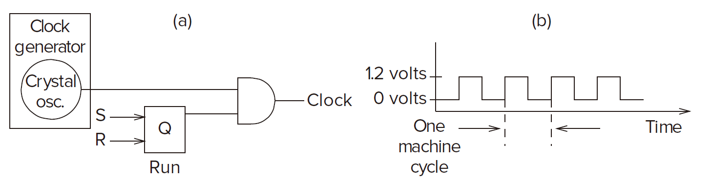
Halting the Computer (TRAP x25)
Stopping the instruction cycle requires stopping the clock.
The clock generator is a crystal oscillator.
Considering the following circuiut, stoppoing the instruction cycle only clearing the RUN latch.
创建日期: 2024.02.21 00:56:50 CST