Appendix
Note
This is the content at the appendix of the book, which serves as a nice supplement as far as I am concerned.
A.3 Interrupt and Exception Processing
The processor can be interrupted by exceptional events.
Interrupt Vector table
x0100 to x01FF Each entry in the table contains the starting address of the service routine handling the needs of the corresponding event. These service routine execute in supervisor mode.
Exception service routine (x0100 to x017F)
It provides the starting address of routines that service events caused by running program itself (internal to the running program).
Interrupt service routine (x180 to x1FF)
It provides the starting address of routines that service events that are external to the running program, such as requests from I/O devices.
Interrupts
The keyboard input interrupts at priority level PL4 and supplies the interrupt vector x80.
Exceptions
The program is trying to do something that is not allowed to do. LC-3 ISA specifies three excecption conditions. - privilege mode exception - attempt to execute RTI in user mode - illegal opcode exception - attempt to execute the instruction having the unused opcode 1101 - access control violation exception, ACV exception - attempt to access privileged memory in user mode
Exceptions are handled as soon as detected.
In many cases, the exception service routine can correct problem caused by the exceptional event and then continue processing. In those cases, the last instruction of the exception service routine is RTI. But in some cases, the exceptional event is sufficiently catastrophic that the exception service routine removes the program from futher processing.
Interrupts and Exceptions also differ in the priority level of the processor during execution of the service routine.
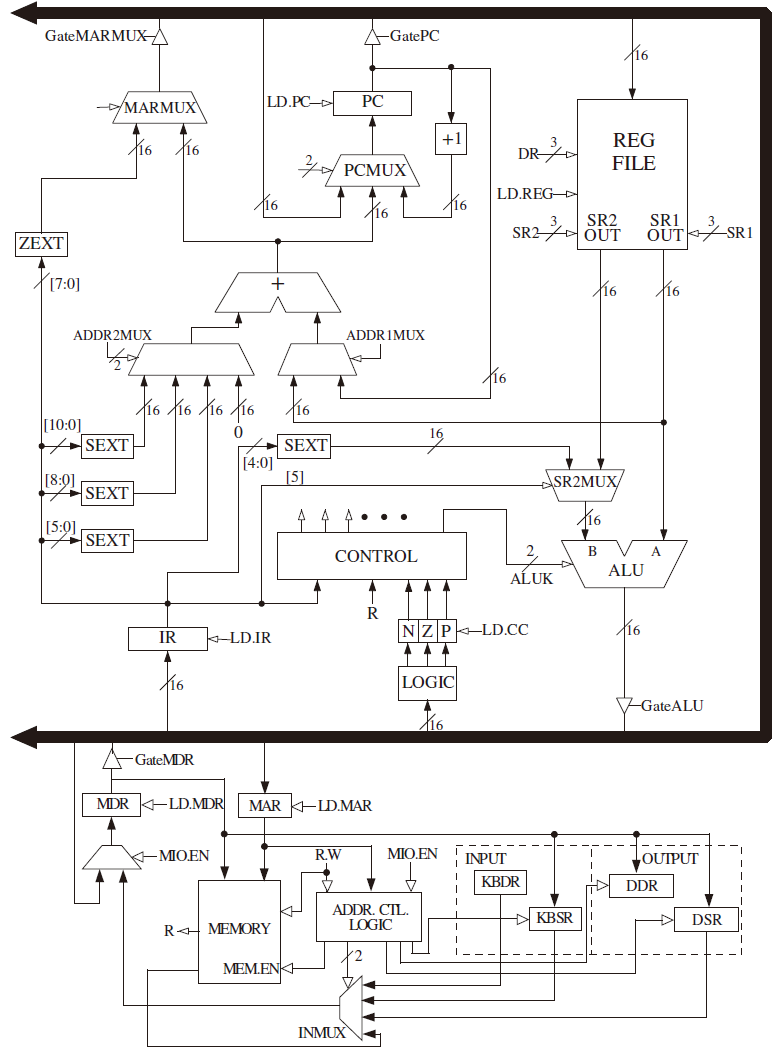
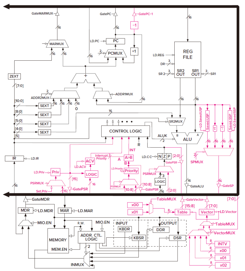
Appendix C. The Microarchitecture of the LC-3
C.1 Overview & C.4 The Control Structure & C.6 Memory-Mapped I/O & C.8 Control Store
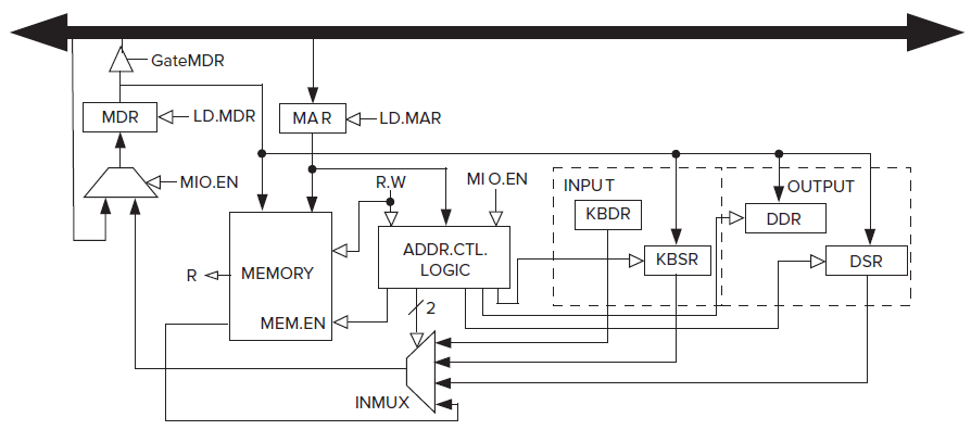
The two main components of a microarchtecture: the data path and the control.
Time is divided into clock cycles.
Each clock cycle, the 52 control signals control both the processing in the data path (42 bits) and the generation of the control signals for the next clock cycles (10 bits).
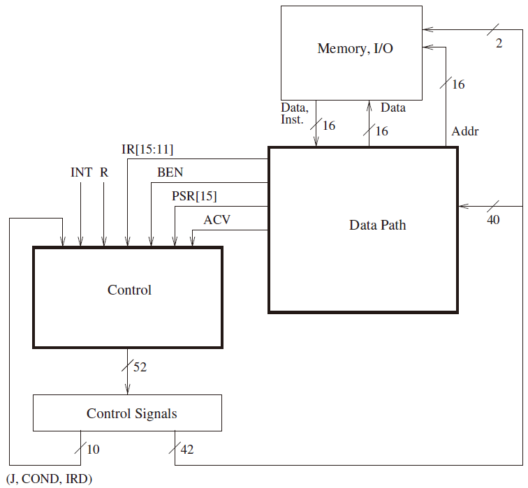
Control Structure
The control structure of a microarchitecture is specified by its state machine.
The 52 control signals specify the state of the control structure of the LC-3 microarchitecture.
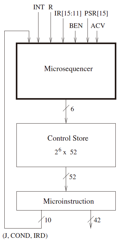
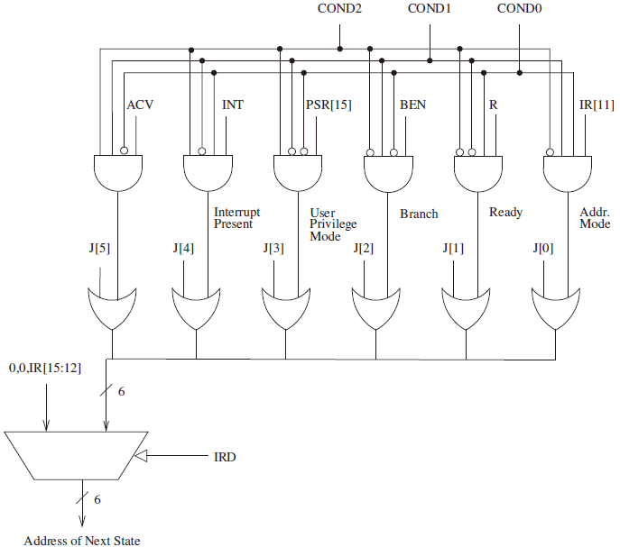
Microsequencer
- J / 6 bits the normal next state
- COND / 3 bits special judge for some conditions
- COND0 Unconditional (not implemented by hardware actually)
- COND1 Memory Ready
- COND2 Branch
- COND3 Addressing Mode
- COND4 Priviledge Mode
- COND5 Interrupt Test
- COND6 ACV Test
- IRD / 1 bit select
0, 0, IR[15:12]when in DECODE phase / state
Control Store
A special memory. Its input is 6 bits to specify a distinct state and its output is 52 bits to specify the corresponding next state. The following file is the Control Table by me. Maybe there are some miskates, and feel free to point out!
Microinstruction
The 52-bit output of the control store is the microinstruction.
Additional Logic
To provide control signals that are not shown in the data path.
Logic to process setCC() (I guess)
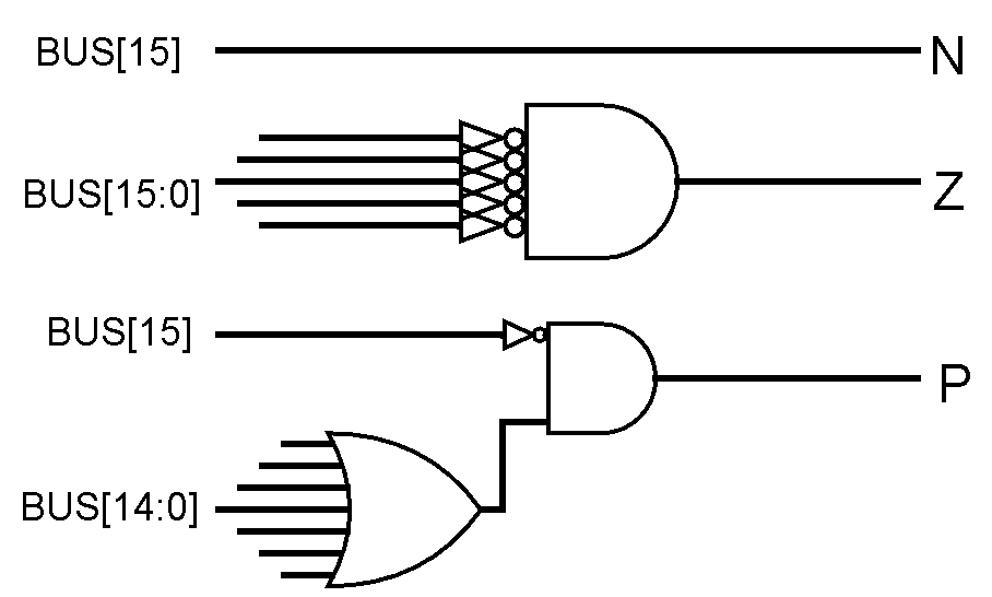
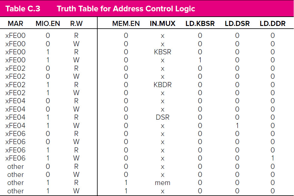
Address Control Logic (ADDR.CTL.LOGIC)
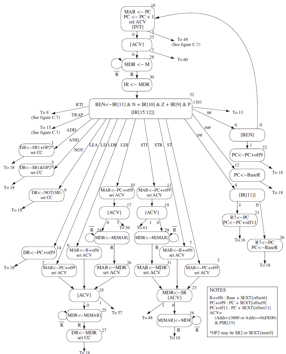
C.2 The State Machine
state machine The graph consists of nodes and arcs.
Each node in the state machine corresponds to the activity that the processor carries out during a single clock cycle.
The state machine which implements the LC-3 ISA requires 59 distinct states to implement the entire behavior of the LC-3. 31 of them are shown in Figure C.2 and 28 of them are shown in Figure C.7.
But the unused state is not state 60, 61, 62, 63. Actually, state 50, 58, 62, 63 are not used due to the detail of the implementation.
6 state variables are needed to uniquely specify 59 states.
Memory acess can take multiple cycles, these states continues to execute until a ready signal from the memory (R) is asserted, indicating that the memory access has completed.
C.3 The Data Path
The data path consists of all components that actually process the information during each clock cycle.
C.5 The TRAP Instrcution & C.7 Interrupt and Exception Control
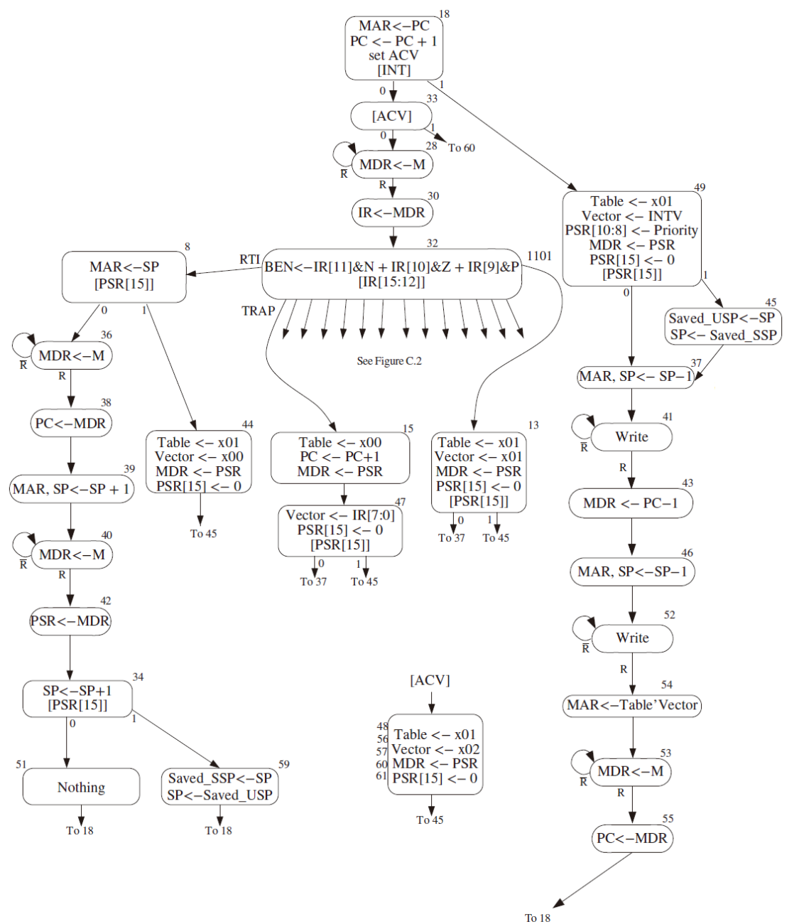
Some abbreviation
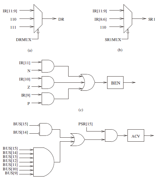
ACV stands for Access Control Violation INT stands for Interrupt Signal BEN stands for Branch Enable
Some comments
Why not put state 15 and state 47 together in one state?
 Because in state 15 MDR <- PSR occupies the global bus, and in state 47, Vector <- IR[7:0 occupies the global bus. The global bus can only be occupied by one data transfer at one clock cycle.
Why PSR[15] <- 0 and [PSR[15]] can be put in one state?
 Because 0 is written into PSR[15] at the end of the clock cycle, but the value tested in [PSR[15]] is read at the start of the clock cycle.
Why PC <- PC + 1 in state 15?
 For state reusage. Since PC minus 1 is stored in the state 43. PC <- PC + 1 serves as an offset.
创建日期: 2024.02.21 00:56:50 CST