Chapter 3 | Digital Logic Structures
Transistor
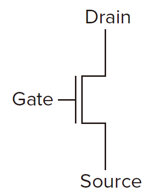
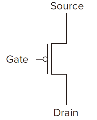
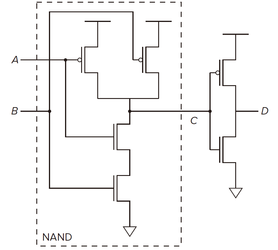
MOS transistor. MOS stands for metal-oxide semiconductor.
A transistor has 3 terminals, the gate, the drian and the source.
Property for N-type transistor
if the gate is supplied with 1.2 volts, the connection from source to drain is a short circuit.
if the gate is supplied with 0 volts, the connection from source to drain is an open circuit.
Property for P-type transistor
if the gate is supplied with 0 volts, the connection from source to drain is a short circuit.
if the gate is supplied with 1.2 volts, the connection from source to drain is an open circuit.
Logic Gates
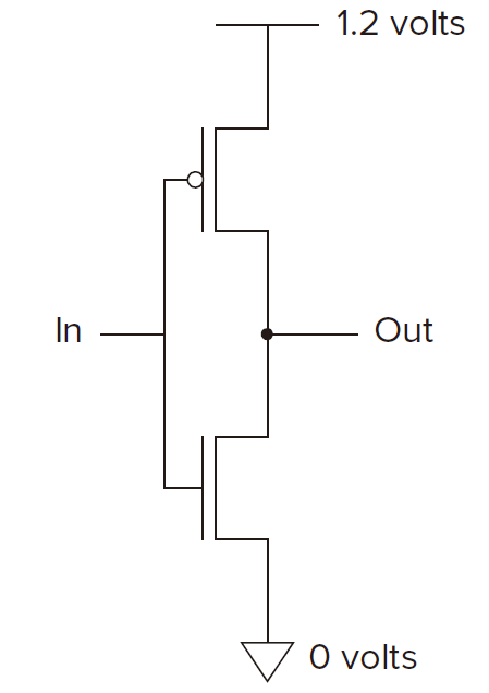
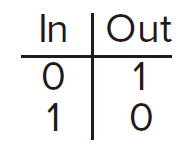
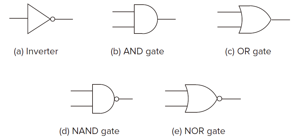
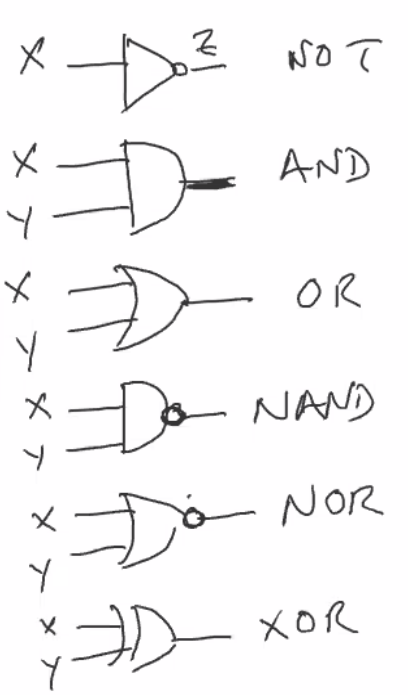
The NOT Gate (Inverter)
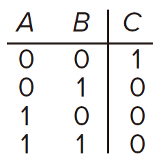
The OR and NOR Gates
NOR for NOT-OR
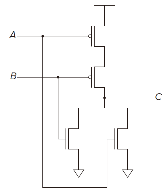
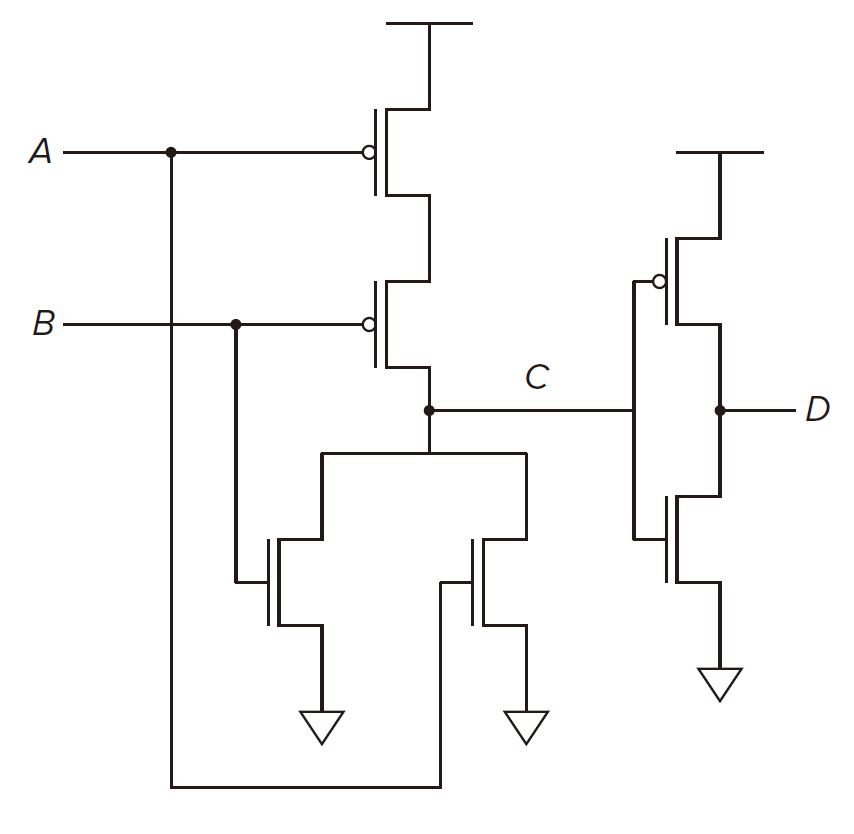
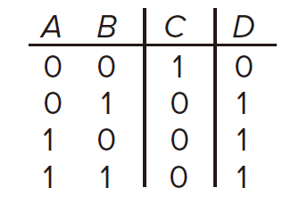
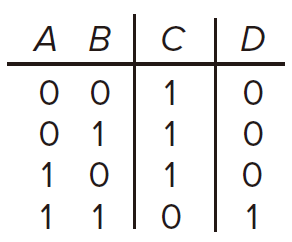
The AND or NAND Gates
NAND for NOT-AND
standard symbols of basic logic gates
Combinational Logic Circuits 组合逻辑电路
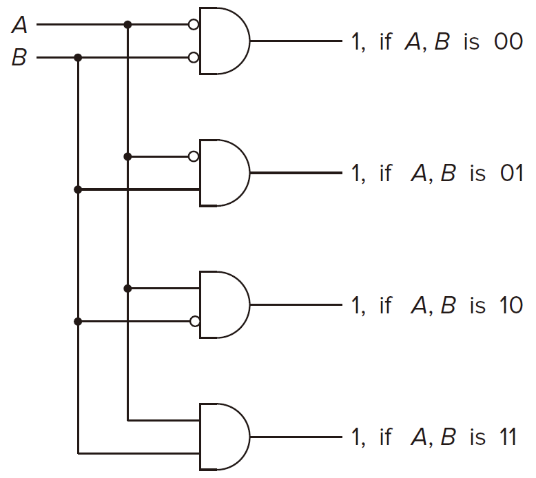
Decoder 译码器
The output line that detects the input pattern is asserted.
In general, decoders have \(n\) inputs and \(2^n\) outputs.
Function To decode how the software ask hardware to do.
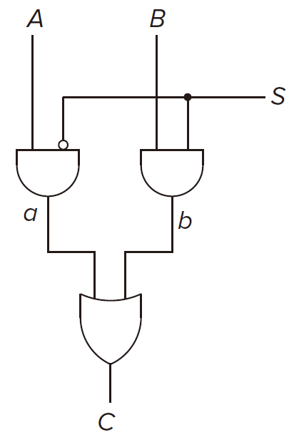
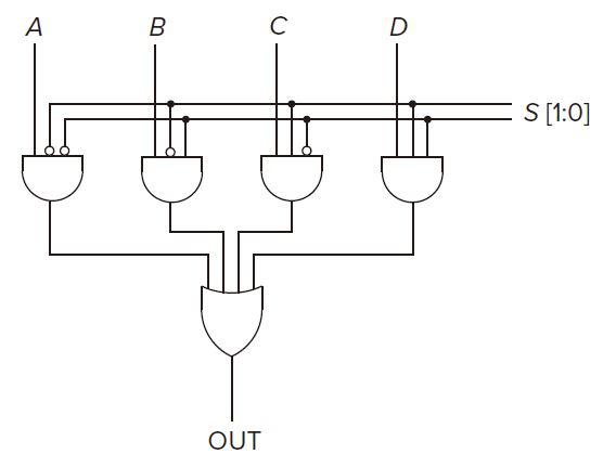
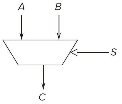
Mux(multiplexer) 多选器
In general, a mux consists of \(2^n\) inputs and \(n\) select lines.
Function select one of the inputs and connect it to the output.
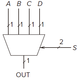
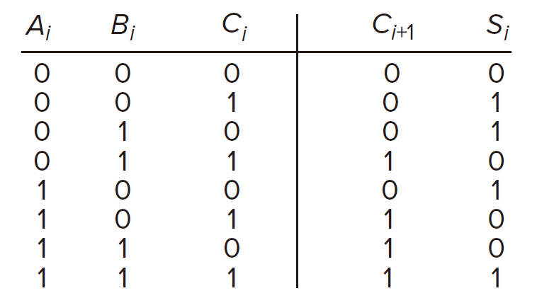
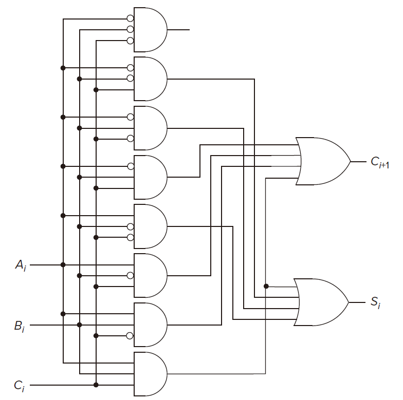
A One-Bit Adder (a.k.a a Full Adder)
\(A_i\), \(B_i\) are the two oprands of \(A\) and \(B\) . \(C_i\) is the carry from the previous column.
\(S_i\) is the sum bit. \(C_{i+1}\) is the carry over to the next column.
Also known as a full adder. But a half adder doesn't consider the carry from the previous column.
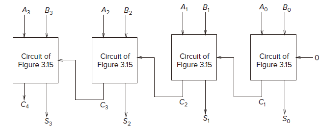
A circuit for adding two 4-bit binary numbers
Other Concepts
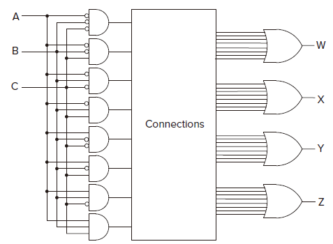
The Programmable Logic Array (PLA) 可编程逻辑阵列
PLA is a building block for implementing any collection of logic functions one wishes to implement.
For n-input logic functions, we need a PLA with \(2^n\) n-input AND gates. The number of OR gates corresponds to the number of logic functions we wish to implement.
The connection is dependant on our wishes. Hence the notion of programmable. We say we program the connections from AND gates outputs to OR gate inputs to implement our desired logic functions.
Logical Completeness 逻辑完备性
If any logic functions can be implemented by a set of gates \(\Omega\), we say \(\Omega\) is logically complete.
\(\Omega = \{\mathrm{AND}, \mathrm{OR}, \mathrm{NOT}\}\) is logically complete.
\(\Omega = \{\mathrm{NAND}\}\) is logically complete. Since two NAND gates can implement a NOT gate. Thus AND gate can be implemented and thus OR gate can be implemented. So as to \(\Omega = \{\mathrm{NOR}\}\).
Basic Storage Elements
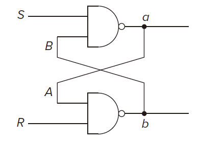
The R-S Latch R-S 锁存器
The value of a R-S latch is the value of the \(a\) point.
S for SET, R for RESET.
SET means to store the value 1, RESET means to store the value 0.
The Quiescent State
S and R are at 1. And the value, either 0 or 1, is storaged.
Setting the Latch to 1 or 0
The latch can be set to 1, if keeping R at 1, momentarily setting S to 0.
The latch can be set to 0 or say clear, if keeping R at 0, momentarily setting S to 1.
In order for the R-S latch to work properly, both S and R must never be allowed to be set to 0 at the same time.
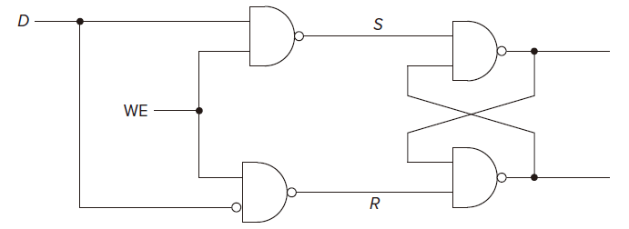
The Gated D Latch D 锁存器 / Data Flip-flop D 触发器
The two additional NAND gates allow the latch to be set to the value of D, but only when WE is asserted.
D for data.
WE stands for write enable(写使能) goal or we can say it the gating singal.
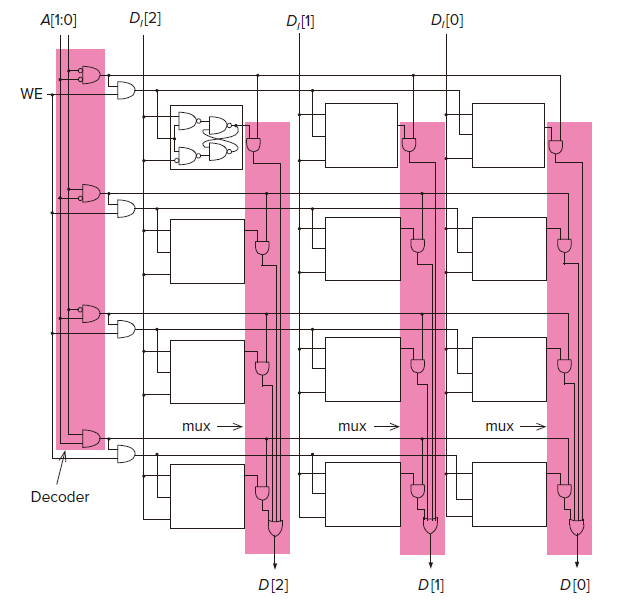
The Concept of Memory
Address the unique identifier associated with each memory location.
Addressability the number of bits of information stored in each locaiton.
Address space the total number of uniquely indentifiable locations.
n bits of address can uniquely identify \(2^n\) locations.
A[high:low] numbers the bits of address and data from right to left, in order, starting with the rightmost bit 0.
[high:low] means a sequence of \(high - low + 1\) bits. (left is high, right is low)
e.g. if A = (1001 1100)2, then A[2:1] = (10)2, A[7:5] = (100)2.
word line one output of memory. In the following diagram example, the unique 3-bit word is the word line.
Sequential Logic Circuits 时序逻辑电路
Finite State Machine
A finite state machine is at the heart of the computer. It controls the processing of information by the computer.
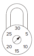
An Example: Combination Lock
The Lock can only be unlocked provided the order R13 - L22 - R3.
State Diagram / State Machine
Definition
state is each of the situation of a system.
current stateis the state the system is coming from.
next state is the state it is going to.
The state of a system is a snapshot of all the relevant elements of the system at the moment the snapshot is taken.
arc is the arrrow in the state diagram.
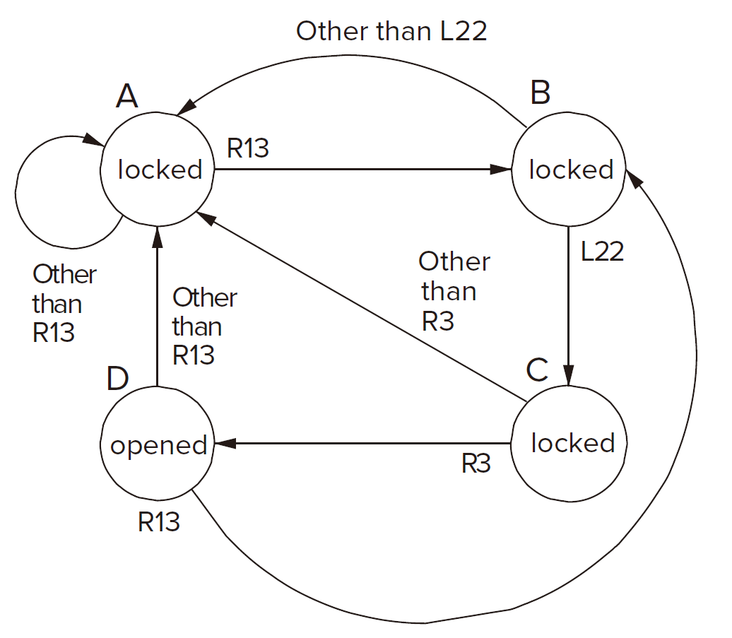
Supplement of the diagram : Add an arc from C to B with the move R13 and modify the arc from C to A with the move Other than R3 or R13. Then we get the complete diagram.
Synchronous Finite State Machine
The example of combination lock above is asynchronous because there is nothing synchronizing when each state transition must occur.
Computers are synchronus because the state transitions take place, one after the other, at identical units of time. They are controlled by a synchronous finite state machine.
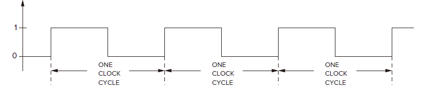
The Clock
clock cycle is each of the repeat sequence of identical intervals. A clock cycle starts when the clock signal transitions from 0 to 1 and ends the next time the clock signal transition from 0 to 1.
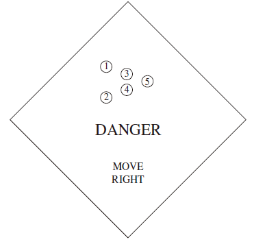
An example : A Danger Sign
If the switch is on, the danger sign flashes from right to left (the first second, 1, 2 are on; the next second, 1, 2, 3, 4 are on; the next, all are on; the next, all are off. It turns in a cycle).
If the switch is off, the danger sign is off.
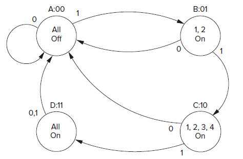
We use 00, 01, 10, 11 to represent different states.
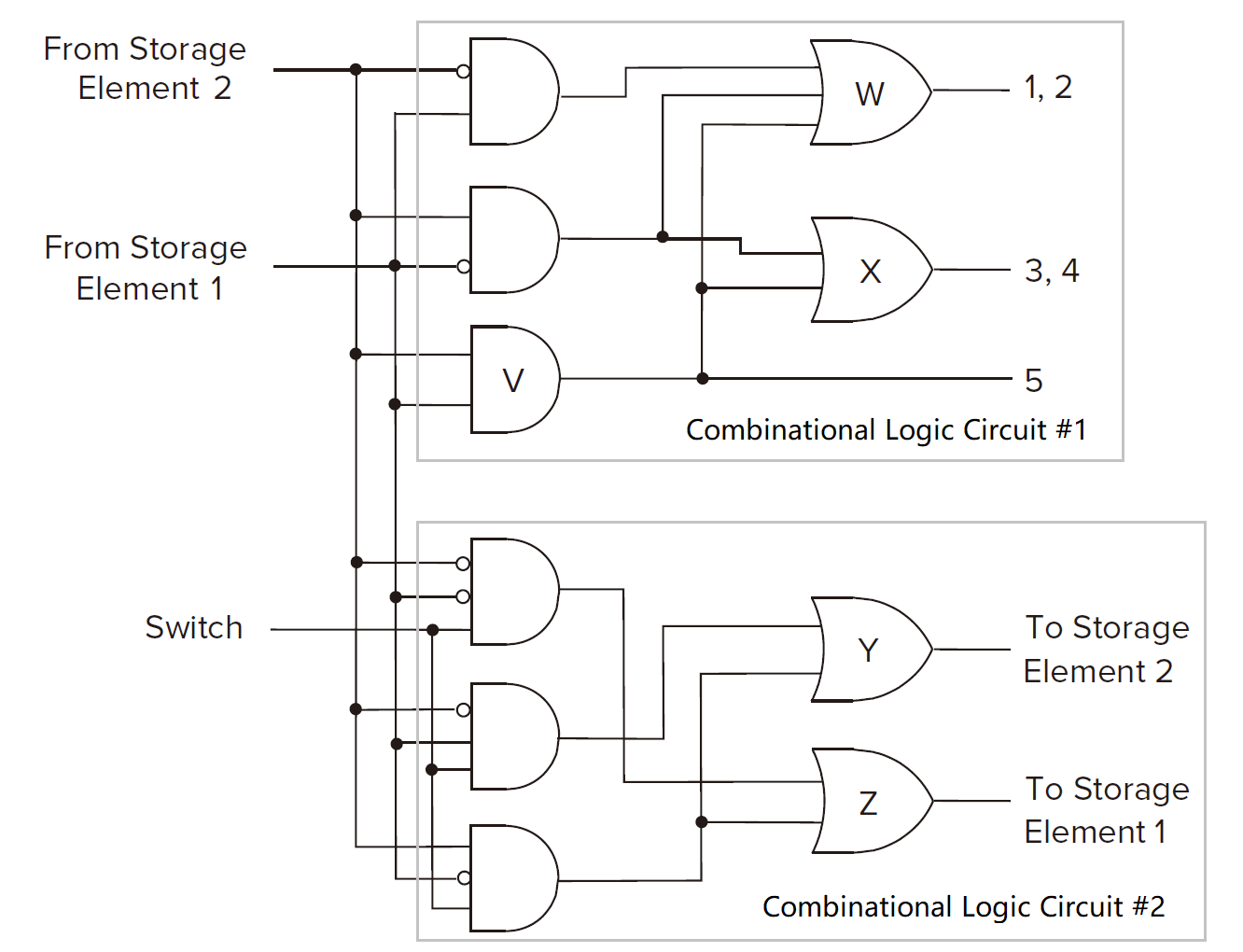
The Sequential Logic Circuit for the Danger Sign Controller
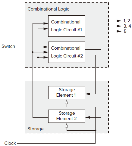
Combinational logic circuits
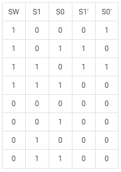
SW for switch. S1 and S0 for the current state. S1' and S0' for the next state.
A problem
If we use gated D latch to storage data, the state of elements would change so fast or maybe asynchronously in a clock circle but not change only once.
Flip-Flop 触发器
It's to replace the gated D latch to storage data synchronously.
Function
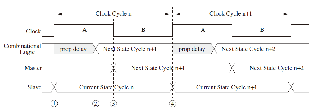
reading and writing a particular variable. Reading must be allowed throughtout the clock cycle, and writing must occur at the end of the clock cycle.
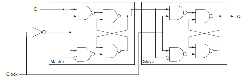
An implementation of flip-flop : master/slave flip-flop 主从触发器
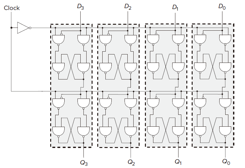
Register
A register is simply a set of n flip-flops that collectively are used to store one n-bit value.
One way to implement registers is with master/slave flip-flops.
创建日期: 2024.02.21 00:56:50 CST